Richard A. Soref: On pioneering silicon photonics
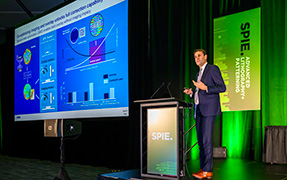
At this year’s SPIE Photonics West symposium, a three-day conference track was devoted to silicon photonics, the material platform for photonic integrated circuits (PICs). Hundreds of talks—ranging from the design of photonic circuits and devices to quantum dot light sources and everything in between—were testament to the field’s growth and attraction, particularly with the rise of data- and power-hungry applications like artificial intelligence.
And that was just one conference this year among many others to be held the world over. After more than 40 years of research and development, silicon photonics has moved from an insight into the optical properties of silicon to commercial production of millions of devices each year that are used mainly as communications transceivers in data centers.
But it would be an understatement to say the future of silicon photonics is bright. With rapidly developing capabilities that include such feats as wavelength multiplexers generating 256 wavelengths of light on a single chip, rapid development for advances in computing, sensing, lidar, and more are not only probable, they are also urgently needed to resolve data processing bottlenecks at much lower energy costs.
Richard A. Soref, the “founding father of silicon photonics,” sees the demand for silicon photonics soaring from millions to billions of devices. Take his word for it. His innovations and decades of basic and applied research in the field have often provided the guideposts for academic research and industrial development.
Soref’s stature in the silicon photonics community began with a series of papers he authored starting from the mid-1980s to the early ’90s. “Early on, I proposed and drew a picture of the archetypical device-laden opto-electronic integrated circuit, which some people call EPIC [electronic-photonic integrated circuit]. I knew that wafer scale E + P would be a terrific ‘marriage’ of two technologies.”
His early research established silicon as a viable platform for PICs, and Soref pointed out that silicon also had a well-established manufacturing infrastructure. His first paper on the topic, published in Electronics Letters in 1985, was titled “Single-crystal silicon: a new material for 1.3 and 1.6 μm
integrated-optical components.”
Of the initial series of papers on silicon photonics, he says, “I presented a detailed vision of a new, mostly monolithic technology in which waveguided on-chip modulators, switches, photodetectors, and laser diodes, working at room temperature, were interconnected along with a variety of ‘passive’ splitters, combiners, filters, polarizers, etc.—all working together synergistically.”
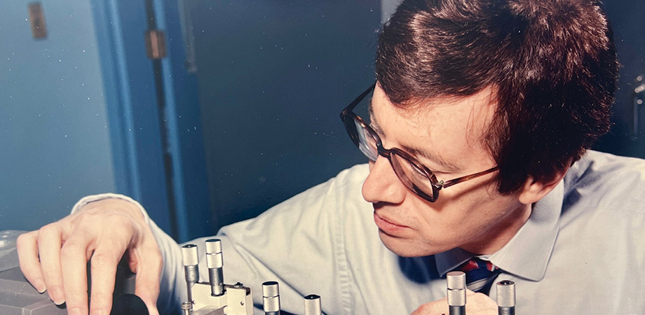
Before he invented silicon photonics, Soref says he knew that there were semiconductor devices fulfilling the lasing and detecting missions of chips for fiber-optic transceivers, but he found them to be clumsy, exotic, and expensive. “When I realized that silicon is highly transparent at the 1,550-nanometer fiber-optic telecom wavelength, I visualized a more elegant and simpler, cost-effective chip that would be beautifully functional, provided that I could propose low-loss waveguides that would sew everything together.”
His vision indeed laid the groundwork for using silicon-on-insulator (SOI) waveguides, now standard in the industry. What’s more, he demonstrated free-carrier electro-modulation effects in silicon that underpin many modern silicon photonic modulators and switches.
Soref says he considers himself partly a materials scientist who is always looking to discover and exploit material properties. But he likewise has been drawn to photonics: “The science of light has always held deep interest for me.”
His love of science began early in life. He tells the story of a roundtrip drive from Milwaukee to Chicago (courtesy of his mother), which allowed 13-year-old Soref to become the youngest radio amateur in the state of Wisconsin. The determined boy—who was fascinated with the vacuum tubes, antennas, and other electronics paraphernalia of the amateur radio scene—had aced an exam testing his knowledge of ham-radio equipment and Morse code.
Soref says Federal Communications Commission examiners in the Windy City told him, “We used the word elephant encoded as E, L, E, F, A, N, T, and you wrote down exactly what we sent you.”
It was, Soref says, the beginning of a lifelong devotion to scientific research, basic and applied, with a particular love for physics.
After completing his PhD in electrical engineering at Stanford University in 1964, Soref says he eschewed narrowly defined career paths in academia or industry. He did stints at MIT’s Lincoln Lab, the Sperry Research Center, and, in 1983, the US Air Force Research Laboratory (AFRL).
After he joined AFRL, Soref says he found the government lab environment to be more challenging in terms of the logistics for experimental work. “As a result, I began to phase out my personal experiments, although I started collaborations with other experimentalists in the United States who could realize devices in their own labs. This continues to the present.”
Along with pioneering silicon photonics, Soref is widely recognized for work developing electro-optical switching, innovations in phase-change materials for switching, contributions to optical matrix switching, advancing midinfrared photonics, nonlinear optics, microwave photonics, and many theoretical contributions.
“All along, I have always enjoyed theoretical physics,” Soref says. “Over the years, I gave many lectures at conferences, but teaching in a classroom has never been my desire or my forte.” And so it was that he reached a research-focused agreement with the dean of engineering at the University of Massachusetts, Boston, to become a research professor there, a position he still holds.
Soref says his outlook for silicon photonics is that it will contribute strongly to future VLSI (very large-scale integrated) photonic quantum computers and photonic neuromorphic computers, where both operate entirely at room temperature. He says wearable biomedical sensors will be big applications as well as 3D imaging and lidar.
In a 2023 review of the field of silicon photonics, Soref and co-authors write: “We have made big leaps in silicon photonics—from building the first high-confinement waveguides and the very first modulators only a couple of decades ago—to a technology that has strategically leveraged materials, integration, and packaging techniques from the CMOS industry to become the dominant technology in the transceiver space. At the same time, silicon photonics is still very much a technology in development, and a gamut of possibilities…signify the prospects that lie ahead.”
William G. Schulz is the Managing Editor of Photonics Focus.