What's next for AR headset display technology?

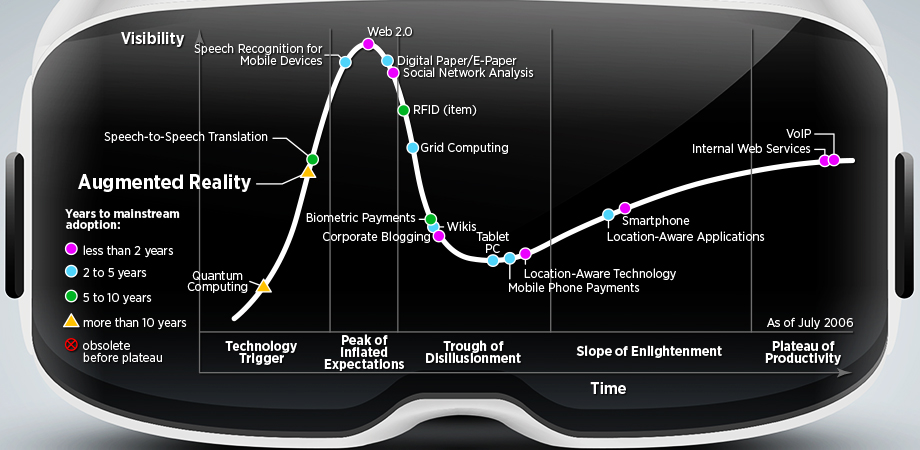
Despite the recent surge in interest, augmented reality (AR) is not new technology. It first emerged half a century ago in the defense sector with holographic combiners for head-up displays. Since that first introduction, it has been a technology featured in almost every vision of the future. It entered the Gartner Hype Cycles in 2006, the same year Apple introduced us to smartphones with the iPhone. It is the longest living technology still in the cycle, spanning more than a decade. Not many technologies can boast such a long and steady path along the twists and turns of the hype cycle. Remaining in the cycle for so long is neither a token of exception nor a token of failure; rather, it relates to the maturity of the underlying market (use cases) rather than the maturity of the technology itself (hardware and software).
There have been impressive advances in both the hardware architectures and technologies for AR and its close relative VR over the past five years, with the pace of developments increasing. At the heart of these improvements is the need to find an effective way to overcome both comfort and immersion challenges. The path to this goal is through improved hardware architectures and software developments that can adapt to the specific limitations of the human visual perception system.
In order to finally reach the "plateau of productivity" and leave the hype cycle, engineers must find an optical design solution to deliver a headset that excels in three keys areas—wearable, visual, and social comfort—without a compromise in the users' immersion experience with display, sensing, and interaction.
"Matching the specifics of the display architecture to the human visual perception system is key to reducing the constraints on the hardware to acceptable levels, allowing for mass production at reasonable costs," says Bernard Kress, principal optical architect at Microsoft.
Dealing with optical complexity
The AR headset is a much more complex device than its VR brother because of the need to augment reality with a holographic image. "You cannot have anything in front of your eyes," Kress explains. "You need the display engine somewhere on the side, and then the optical combiner merges the reality you see with the digital image, and superimposes this accurately on the reality, a technique called spatial anchoring.
"If your digital image is a pink elephant and you have an armchair in front of you, then you want to anchor the pink elephant on your armchair in your living room. That pink elephant looks like it is there, but it is just a hologram. The task for the AR is to scan the reality and know that there is a chair and then align very accurately the digital information with the reality so that the pink elephant looks like it is sitting in your armchair.
The display engine is the main optical building block of the display architecture of any HMD and its role is threefold. It must produce the desired image (usually in the angular spectrum), provide an exit pupil overlapping with the entrance pupil of the optical combiner, and shape this exit pupil to the aspect ratio required by the pupil expansion scheme to create the desired eyebox, the 3D region located between the combiner and the human eye pupil over which the entire field of view is visible for a typical pupil size.
Display engines are usually formed around three distinct building blocks. There is the illumination engine (for non-emissive display panels), the display panel (or micro-display) or scanner, and the relay optics (or imaging optics) that form the exit pupil for the combiner optics.
When it comes to display engines for AR headsets, there are competing technologies: microLEDs and laser-based scanners. Kress elaborates: "There are two types of panel display systems available for VR and AR systems today: direct-view panels and micro-display panels," he explains. "The former is used in smartphone systems (LTPS-LCD, IPS-LCD, or AMOLED) and range in size from 3.5–5.5 inches and in resolution from 500–850 DPI. Micro-display panels, on the other hand, come in sizes from 0.2–1.0 inches and in resolution from 2000–3500 DPI."
MicroLEDs use exceedingly small LEDs that combine red, green, and blue subpixels to reproduce a color. MicroLEDs offer the potential for significantly higher brightness, as well as enhanced robustness and longer lifetime. In addition, a major advantage is greater efficiency, which can mean significantly reduced power consumption, making the technology ideal for battery-powered products. Their small form factor also makes microLEDS ideal solutions for products such as head-mounted displays, like AR and VR headsets.
With laser-based scanners, on the other hand, a microelectromechanical system (MEMS)-based collimated light scanner scans a holographic element (HOE) that is embedded in the lens of the device. This HOE redirects the light beam onto the human retina surface, directly painting a picture that is always in focus.
Manufacturing challenges
Although there is a mounting sentiment within the photonics industry that microLEDs could have a big role to play in display engines of the future, there are still challenges with developing methodologies to fabricate and assemble small LED devices. Not least of these is manufacturing and the challenge of epitaxy.
Epitaxy refers to a type of crystal growth or material deposition in which new crystalline layers are formed with one or more well-defined orientations with respect to the crystalline substrate. When the wavelength and thickness are uniform, the wavelength is more concentrated, and the backend inspection cost of the epitaxy maker can be greatly reduced. If the LED chip is reduced to less than 100 micrometers, then power leakage may occur due to nonuniformity caused by the cutting damage around the LED chip, which may affect the overall luminescence characteristics.
According to Anne Corning of Radiant Vision Systems, microLEDs have required the display industry to develop entirely new production assembly technologies, as they use different die structures than traditional LEDs or OLEDs and require new manufacturing infrastructure.
"A microLED screen is composed of millions of tiny pixels in chip form, each of which can be monochromatic or contain some combination of red, green, blue and/or white subpixels," Corning says. "To fabricate a display, microLED wafers must be created via high-yield epitaxial growth. Then each individual wafer must be transferred to a substrate or backplane that holds an array of units in place.
"Methods such as elastomer and electrophotographic transfer, roller transfer, and fluid assembly are being tried. Researchers are also working to resolve the challenges associated with integrating compound semiconductor microLEDs with silicon-based integrated circuit devices that have vastly different material properties and fabrication processes."
Coming of age
According to Nick Cherukuri, CEO of enhanced reality specialists ThirdEye, microLEDs will become the norm for AR displays within the next five years. "They are the ideal AR/VR display technology due to its method of high-density blue microLEDs and then patterning red and green dots over two-thirds of the display," he says. "microLEDs are extremely attractive, and with all the engineering efforts being spent on this, the cost issue should be overcome. With laser-based scanners we have seen a reluctance from end users to this type of technology due to it projecting into the user's eyes. We anticipate microLEDs to become the dominant display technology within five years."
It is a sentiment echoed by Alice Ramsden de Gómez, consumer product manager at Epson UK. "Both microLED and laser-based scanners have high brightness potential. However, both have technical issues in the display performance, such as crystal defects, eye box size, and speckle patterns," she says. "Epson believes these issues make it difficult to fully meet customer expectations. Many companies have been improving both technologies to solve these issues and we are paying close attention to how these influence future trends.
"Currently OLED is a superior solution to both of these technologies, particularly in terms of display quality, however we believe microLEDs will become one of the best solutions in the near future because it has the potential for higher brightness than OLED and higher display quality than laser-based scanners."
It is anticipated that the growing scope of applications across different industries, such as medical, retail, and automotive, will drive the demand for AR. According to a 2020 report from QY Research, the global augmented reality market size is projected to reach $3.6 billion by 2026, up from $849 million in 2019, at a CAGR of 27.6 percent during 2020–2026. But before any of this is realized, the technology still needs improvement. The ability to increase production and quality of microLEDs will ultimately play a huge role in whether LBS or microLEDs are the preferred display engines in AR. Meanwhile, engineers will continue refining designs for the next generation of HUDs to find the perfect mix of technology, comfort, and style to break out of the hype cycle and truly deliver on the promise of AR.
Mark Venables is an award-winning technology writer who has covered science, innovation, and transformational technology for leading newspapers and magazines for over 25 years.
Related SPIE content:
Hear from x-reality hardware experts in the SPIE AR/VR Fireside Chat Series
| Enjoy this article? Get similar news in your inbox |
|


