From PIC to probe

Similarly as for electronics, photonic circuits can be miniaturized onto a chip, leading to a so-called photonic integrated circuit (PIC). Although these developments are more recent than for electronics, this field is rapidly evolving. One of the main issues, however, is to turn such a PIC into a functional device. This requires optical packaging and coupling strategies to bring light into and to get light out of the PIC. For example, for optical communication a connection needs to be made with optical fibers, which then transport the light pulses over long distances. Alternatively, the PIC could house an optical sensor which requires external light for its readout. Since light on a PIC propagates in very tiny channels with sub-micrometer dimensions, called waveguides, this optical coupling is very challenging and requires careful alignment between the PIC and external components. The optical components are also very fragile, so that proper packaging of the PIC is vital to result in a reliable device.
The research team of Prof. Van Steenberge and Prof. Jeroen Missinne at Ghent University and imec is developing solutions to overcome the packaging and integration challenges related to PICs, for next-generation telecommunication systems, sensors, and biomedical devices. One of their activities is focused on using very small lenses (microlenses) to more easily connect the optical channels on PICs with external optical fibers or other elements. They have demonstrated microlenses that can be integrated on the PIC itself, during its fabrication process or external microlenses that are added during the packaging process. The latter is the topic of a recent paper in the Journal of Optical Microsystems.
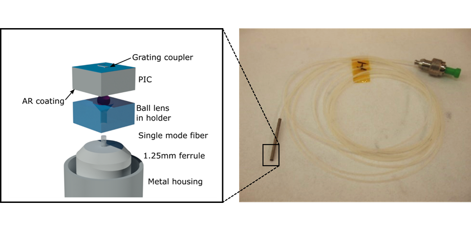
A small ball lens with a 300 um diameter was used to make an efficient connection between a sensor on a PIC and an optical fiber which can be connected to standard readout equipment. In addition, the paper describes the import steps that were needed to transform the PIC into a functional and fully packaged miniature sensor probe (less than 2 mm in diameter). The type of optical sensor that was developed in this demonstration was a Bragg grating temperature sensor that could measure up to 180°C.
The sensor was realized in the framework of the European SEER project together with Argotech (Czech Republic) and the Photonics Communications Research Laboratory at the National Technical University of Athens (Greece). In this project, several European partners focus on integrating optical sensors in the manufacturing routines for making composite parts such as those used in aircraft, which will ultimately allow process optimization, energy savings, and cost savings.
Read the Gold Open Access article by Missinne et al. “Silicon photonic temperature sensor: from photonic integrated chip to fully packaged miniature probe” J. Opt. Microsys. 4(1) 011005 (2023) doi: 10.1117/1.JOM.4.1.011005.
| Enjoy this article? Get similar news in your inbox |
|


