Augmenting reality through lithography

Augmented reality superimposes a computer-generated image on that of the real world, creating a composite view. To date, doing this for the mass market has proven hard to pull off. Device challenges rooted in optics are one reason why. Advances in lithography, though, could eliminate some of those problems, according to two separate presentations at the 2023 Advanced Lithography + Patterning conference.
In the first talk, Richard Farrell, an integration engineer at Meta Reality Labs, discussed AR combiners. These devices overlay a computer-generated image with that of the real world, with the idea being to put these devices along with everything else needed into glasses in a format that can handle different head sizes. In addition to being able to meet technical requirements about size and performance, such products also must satisfy another crucial commercial constraint.
“We are in a consumer market and most of us here don’t want to pay a lot for devices,” Farrell said.
To meet this goal for high performance at a low cost, the staff at Reality Labs is investigating and developing wave guides, structures that send light in a preferred direction while keeping it from leaking out in other directions. In the case of a combiner, that means light goes into the eye and not elsewhere. At the same time, combiners must interfere as little as possible with incoming light from the real world.
For these waveguides, the researchers are building structures using nanoimprint lithography. As the name implies, this process involves using a mold to physically impress a pattern into a polymer, with the polymer then cured by light or heat. The next process step frees the polymer from the mold. The patterned polymer can then be used directly in the device or to pattern another material by acting as an etch mask. This second material will then go into the combiner. In his presentation, Farrell discussed using nanoimprint lithography to construct a slanted grating to accomplish this objective.
The researchers are working on various problems, among them how to get the cured polymer free of the stamping mold. This process is made more difficult due to the shape of the slanted grating, which look like repeated long, relatively thin tongues sticking out at an angle of 45o or more. Another issue is the mold itself, which degrades over time due to being in contact repeatedly with a polymer as parts are patterned. While not an issue during testing, this degradation could pose problems in high-volume production.
“To truly deliver this immersive display takes a lot of work,” Farrell said in summing up this research and development effort.
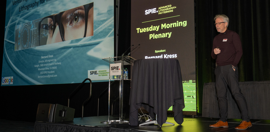
In his talk on pushing the limits of and going beyond nanoimprint lithography, Bernard Kress, director of XR engineering at Google, also noted challenges. These are made more difficult because in optics there is no steady increase in performance and decrease in price as is the case with semiconductors.
“There’s no Moore’s Law in optics,” Kress said.
Nonetheless, optical systems do tend to get smaller, thinner, and lighter through the application of ingenuity and engineering. For instance, one approach is to stack optical elements, with reflection or other means moving the light around. Typically this means that alignment becomes an issue – unless a device is made using an integrated approach conceptually similar to what is done with integrated circuits (ICs). In that case, everything is aligned during manufacturing and it remains aligned. This creates a significant cost savings because the alignment of separate elements in an optical system often ends up being more expensive than the optics, Kress said.
Lithography could be used for such manufacturing, but it faces hurdles. In semiconductor manufacturing there are hundreds of chips on a wafer. For optical components intended for glasses, there may only be a dozen. When these are packaged, there may only be two or three complete final products because there are two eyes and three primary colors involved. The small number of products changes the economics of manufacturing.
The industry is still researching the best lithographic approach, with Kress mentioning nanoimprint lithography, lithographic interference patterning, and other techniques. He also spoke of wet resist, widely deployed in semiconductor manufacturing, and dry resist, also used in making semiconductors.
Currently, there is no clear winning lithography for manufacturing AR optical components, but there also isn’t a need to do high-volume production for a mass consumer market. That could change, though, if and when a compelling consumer use case emerges.
Concluding his talk, Kress noted that right in front of consumer’s eyes is prime real estate for a new use case, one that could drive demand because of new capabilities brought about by technology.
In speaking of the small area right in front of people’s eyes, Kress said, “This prime real estate is poised to become more and more functional.”
| Enjoy this article? Get similar news in your inbox |
|


