Optipedia • SPIE Press books opened for your reference.
Semiconductor Lasers
Excerpt from Field Guide to Lasers
Semiconductor lasers utilize a semiconductor as the gain medium. Most of them are electrically pumped laser diodes, where electron-hole pairs are generated by an electrical current in a region where n-doped and p-doped semiconductor materials meet. However, there are also optically pumped semiconductor lasers, where carriers are generated by absorbed pump light.
Laser devices are fabricated on polished semiconductor wafers with lithographic techniques. Common semiconductor materials for the active regions are GaAs, AlGaAs, GaP, InGaP, GaN, InGaAs, InP, and GaInP. These are all direct bandgap materials, because indirect bandgap materials, such as silicon, do not exhibit significant light emission.
Although semiconductor lasers occur in a great variety of forms, some typical aspects of importance include:
- Electrical pumping with moderate voltages and high efficiency is possible particularly for high-power diode lasers and allows for their use as, for example, pump sources for highly efficient solid-state lasers.
- A wide range of wavelengths is accessible with different devices, covering much of the visible, nearinfrared, and midinfrared spectral region. Some devices also allow for wavelength tuning.
- Small laser diodes allow fast switching and optical power modulation, allowing their use, for example, in optical data link transmitters.
Such characteristics make semiconductor lasers the most important type of lasers, technologically speaking. Their applications are extremely widespread and include optical telecommunications, optical data storage, metrology, spectroscopy, material processing, pumping of other lasers, and medical treatments.
Light Amplification in Semiconductors
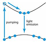
Light emission in semiconductors is usually associated with electronic transitions from the conduction band to the valence band. Optical amplification via stimulated emission is possible for a sufficiently high carrier density in the conduction band. In this situation, electrons near the bottom of the conduction band make transitions to the highest (and depleted) energy levels of the valence band, which can also be described as recombination with holes in the valence band. The photon energy is at or somewhat above the bandgap energy, and this determines the emission wavelength. Optical pumping is possible at a somewhat shorter wavelength and involves the fast relaxation of carriers in both bands. Pumping is also possible with an electrical current sent through a p-n junction; carrier recombination occurs where the p and n materials meet.
Optical gain and efficient laser operation is more difficult to achieve at high temperatures, where the carrier distributions in the two bands are more "smeared out" in thermal equilibrium. Temperature changes also somewhat affect the wavelength of maximum gain—often by roughly 0.3 nm per kelvin.
The achievable optical gain can be quite high (easily 10% in a millimeter) and in some cases even significantly more. However, the required high power density can be applied only to small volumes. Therefore, the light is often tightly confined in a waveguide structure, which also confines the carriers generating the gain. This is called a double heterostructure.
R. Paschotta, Field Guide to Lasers, SPIE Press, Bellingham, WA (2008).
View SPIE terms of use.

